Overview
Light management continues to be of great interest to society, impacting wide-ranging application areas including photovoltaics, displays, quantum devices, thermal regulation, security, healthcare, environmental sensing, and agriculture. Underpinning these emerging technologies are important scientific challenges: optical materials are needed to both meet application demands and reveal new optical phenomena, and we need to understand interactions between materials in complex assemblies and across length scales. We design nanostructures using a combination of experimental and theoretical techniques, synthesize our structures using both bottom-up and top-down methods, characterize the material properties, and ultimately integrate our designs into functional devices and systems. Recent highlights from the Ferry group are shown below.
Scalable manufacturing of nanostructures and metasurfaces
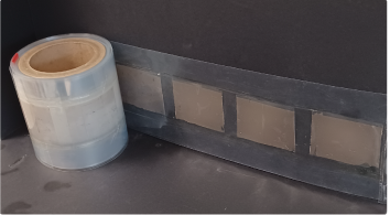
We are interested in developing scalable manufacturing methods and materials for optical applications. Many exciting application spaces for optical nanostructures, metasurfaces, and metamaterials are inherently large-area and/or large volume, including building-integrated materials, aerospace applications, displays, security tagging, and wearable optoelectronics.
Our current work creates scalable, additive nanopatterned surfaces with the same resolution as advanced lithographic processing over m2. This method works for metals, dielectrics, and semiconductor inks, and we have demonstrated it on roll-to-roll lines. The process is additive, so critical materials are used efficiently. Our process utilizes topographical discontinuous dewetting to selectively localize inks in targeted regions, producing large-scale metasurfaces that require very little functional material. Other recent work studies polymer self-assembly for large-scale functional optical materials with tunable optical properties.
Light Management in Optoelectronic Devices
We design nanostructures for light management in optoelectronic devices, with expertise in managing light from the nanoscale to large-scale, outdoor installations. Recent projects include optimization and light management strategies for OLED design, and designing nanophotonic structures for light and thermal management in solar cells and modules. Our systems direct light to areas of the device where they are most critical, and away from detrimental areas. We have also studied the use of sunlight filters for controlled environment agriculture using nanocrystal-polymer composites, where the ability to tailor the incident spectrum for both enhanced crop yield and electricity generation simultaneously addresses food security and energy demands.
Chiral Nanomaterials
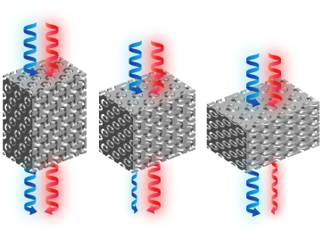
Chirality, the symmetry property of objects that are not superimposable on their mirror image, is ubiquitous in nature and engineering. Nanoscale chiral materials have attracted attention for numerous applications, from sensing to optoelectronic devices to anti-counterfeiting strategies.
Our research group has studied a variety of different chiral materials, including lithographically patterned structures comprised of both plasmonic and semiconductor nanocrystal elements, chiral nanocrystals, and single and double gyroids that can be assembled using block copolymers. Our work has shown various strategies for tuning and switching these materials, by modifying the refractive index of nearby materials, changing ligand-nanoparticle interactions, or controlling the surface structure of single and double gyroid thin films. We have demonstrated a design process for circularly polarized luminescence that consists of both patterned plasmonic structures and patterned quantum dots that achieves simultaneously high photoluminescence intensity and degree of polarization.
Tunable and switchable optical materials

The ability to tune and switch the optical properties of materials is essential for many optical devices, including tunable filters, beam steering, dynamic windows, and others. Our research group is studying electrolyte gating as a route to tunable optics, as part of our MRSEC research. Our recent paper on La1-xSrxCoO3-d (LSCO) measured the complex refractive index before and after electrochemical reduction across a range of compositions, showing significant refractive index modulation across the near and mid-infrared. Operando spectroscopic measurements are powerful tools for understanding mechanisms and endurance in these materials, where recent results demonstrated the cycling limits of LSCO.